Metallography
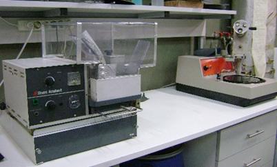
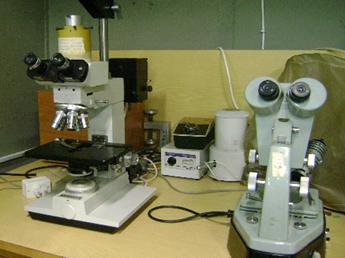
The laboratory is well equipped for the preparation of all types of materials with diamond cutting and polishing (right) for metallographic examinations using optical microscopy (with polarised light if necessary) in combination with Image Analysis software. The maximum usable magnification can reach about 2000X.
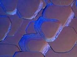
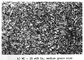
Metallographic analyses using optical microscopy are extremely useful for the determination of different phases in various metallic alloys and ceramic compounds, usually after chemical and physical etching as shown in the microphotos right and below.
chemical etching where the grain
interfaces are clearly visible as well as
some pores (dark)

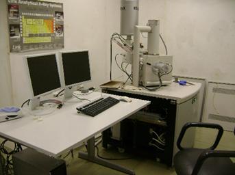
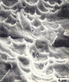
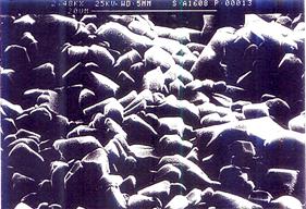
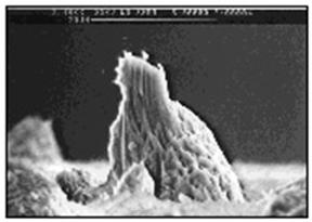
Scanning Electron Microscopy (SEM)
While optical microscopy is used for indentifying of phases after special surface preparation, grinding and pilishing often followed by etching, SEM (right) provides important information on the surface whether polished or fracture. The maximum possible magnifications is close to 200000X.
In combination with the elemental EDX analyser, the SEM is clearly one of the most useful metallographic technique with a very wide spectrum of applications such as fracture analyses, grain crystallisation, interface analyses, contaminations, etc.